Apple I Replica Creation -- Chapter 3: Digital Logic
| Chapter 3 |
| Digital Logic |
Introduction
This chapter provides an introduction to digital logic, which is the basis of microcomputer design. Although it is not critical that you understand everything in this chapter, in order to gain a full understanding of the microcomputer, a background in digital logic is imperative. Don't be afraid to move on if you don't understand a particular section. Each level we'll be covering (digital logic, microcomputer, and software) contains a certain degree of abstraction from the layer following it.
Breadboarding
The experiments in this chapter will all be done using breadboards. To begin, perform the following steps:
- Find a power supply and snip off one of the hard drive connectors.
- Strip down the end of the red wire (5 volts) and the black wire (ground).
- Turn on the power supply and check these cables with your multimeter to ensure that they really are 5 volts and ground.
- On your breadboard, you'll see a series of red and blue lines running the length of the plastic. Connect the power supply cables to the binding posts, then use a couple pieces of spare wire to connect the binding posts to these lines (Figure 3.1).
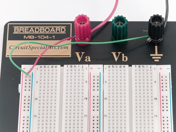
Figure 3.1 Connecting Power and Ground
The holes beside these lines are for power and ground, respectively. A look inside might help us understand how breadboards work (Figure 3.2):
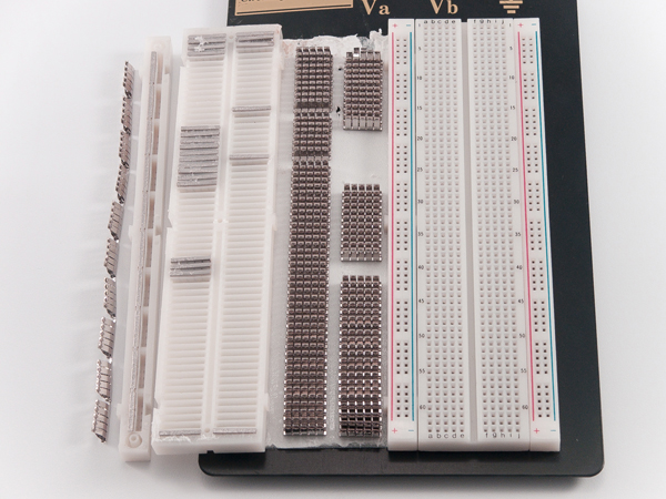
Figure 3.2 Inside the Breadboard
Inside each hole is a metallic socket, into which you can plug a wire or component. Every socket in the ground strip is connected; if you connect one socket to your ground supply, all sockets in the strip are grounded. The same rule applies to the power strip. We have three columns of power and ground strips with nothing connecting them, so we need to use jumper wires across the bottom (Figure 3.3).

Figure 3.3 Jumpering Power and Ground Lines
In order to help gain an understanding of the rest of the board, take a look at Figure 3.2 once again. Each horizontal row of five sockets is linked. Therefore, if we wanted to connect three resistors in a series (one after the other), we could configure them as shown in Figure 3.4.
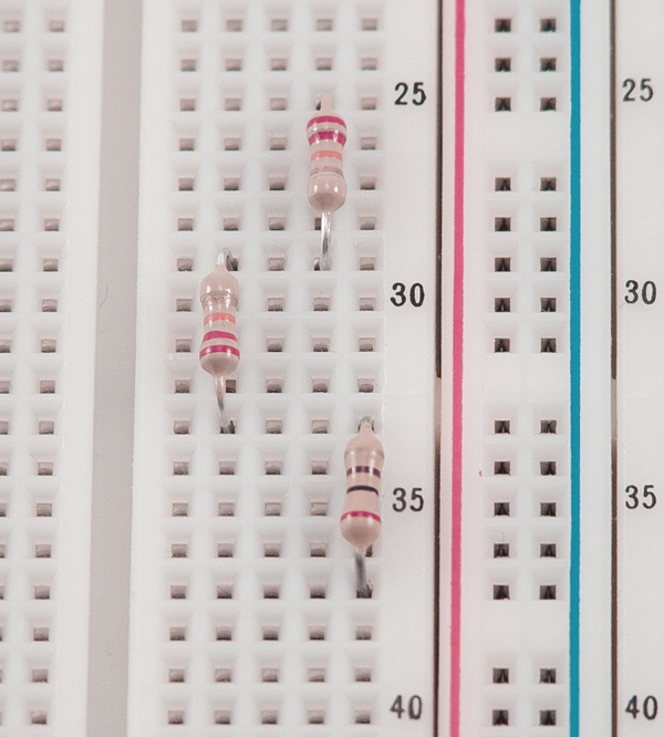
Figure 3.4 Resistors in Series
Next, let's make sure everything's configured correctly by running some tests using a logic probe:
- Connect your probe's alligator clips to the power and ground lines (Figure 3.5).
- Touch the point of the probe to any socket on the power line. The "HI" light should come on.
- Test a socket in each strip by repeating step 2.
- Repeat step 2 yet another time for the ground sockets; for these, the "LO" light should come on (Figure 3.6). The sockets connected to neither power nor ground should produce no light at all.
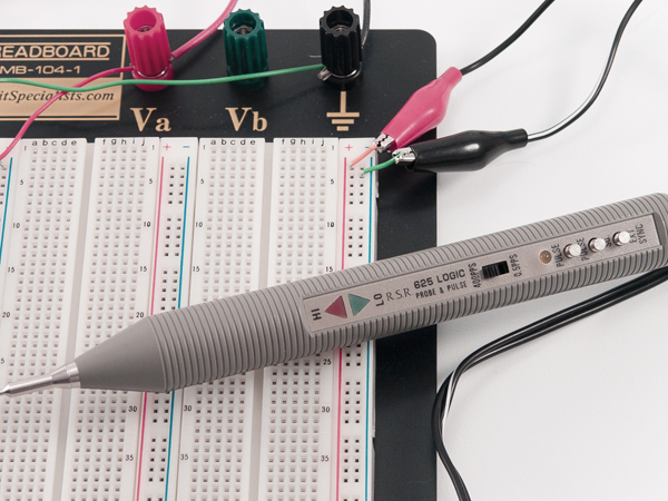
Figure 3.5 Connecting the Logic Probe
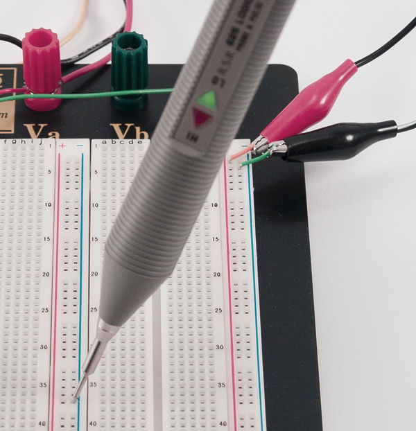
Figure 3.6 Testing with the Logic Probe
Electricity
Next you'll find a very brief, hands-on introduction to electronics fundamentals. In this chapter, I've provided enough of the basics that you shouldn't have too much difficulty completing your Apple I replica; however, a more substantial understanding of electronics will serve you well in the future. If you'd like to do some further reading, The Art of Electronics by Horowitz and Hill (Cambridge University Press, 1989) is the most widely acclaimed book on the topic but is perhaps too difficult for beginners. A more appropriate book for the novice is Hands-On Electronics by Kaplan and White (Cambridge University Press, 2003).
Voltage and Current
Voltage (V) is the potential difference between two points, measured in volts. When you take your multimeter, set it to Volts DC, and touch the probes to the breadboard—negative to negative, and positive to positive—you'll get a reading of 5 volts. That's the amount of energy it takes to move charge from the lower point (ground) to the higher.
Current (I) is used to measure the rate of flow of an electrical charge and can be thought of like the flow of water. Current is measured in amperes or amps (A). Whereas voltage is measured between two points, current measures the rate of flow at a particular point. While DC voltage is steady (hook your circuit up to a 5-volt supply and 5 volts is what you'll get), current only "pulls" as much as is needed. If you have a power supply capable of 10 amps and your circuit only needs 5 amps, then 5 amps is all that it will pull.
Power (P) is voltage multiplied by current. It's measured in watts, which you're probably familiar with seeing on light bulbs. In fact, light bulbs serve as an excellent example. Consider a 20-watt and a 50-watt halogen bulb (Figure 3.7). Both require 12 volts. The difference is in the current, which we can calculate using P=VxI.
I = P / V 20 watts / 12 volts = 1.6 amps 50 watts / 12 volts = 4.16 amps
Appropriately, we see that the brighter light bulb draws significantly more current than the dimmer one.
Exercise: Replace all the 40-watt bulbs in your house with 200-watt bulbs. See what happens to your electricity bill.

Figure 3.7 Light Bulb Circuit
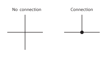
Intersections If you have two wires you want to connect in a schematic, place a large dot at the point of connection. If there is no dot, readers (and the schematic software) will assume there is no physical connection between the two lines. See Figure 3.8 for an example.
|
Resistors and Diodes
Now that we've explained the basics of current and voltage, we can take a more hands-on approach to resistance. Let's wire up a light-emitting diode (LED). A diode is a device that only allows current to flow in one direction. For this experiment, let's use a standard red LED, such as model #276-041 from Radio Shack. These LEDs have a recommended voltage of about 2.25 volts, with a maximum voltage of 2.6 volts (you'll find all of this information on the packaging). The maximum current is 28 mA. Our power supply provides 5 volts; so, if we hook the LED up directly to it, the LED will probably burn out. (If you have a spare, try this!)
To reduce the voltage, use a resistor. A resistor is a partial conductor, usually made of carbon. We can calculate resistance using the equation:
R = V / I
where R (resistance) is calculated in Ohms, V (voltage) in volts, and I (current) in amps.
Our circuit is shown in Figure 3.9. Since we have 5 volts being supplied, and our LED uses 2.25 volts, that leaves 2.75 volts that we need to have a resistor take care of. 2.75 is the value we want to use for V in this equation. Now we can calculate:
R = (5V – 2.25V) / .028 A = 98 Ohms
If you calculated decimal places, you're taking these numbers too seriously. Next, we need to find a 98-Ohm resistor. A resistor with a smaller value will provide less resistance and potentially allow damage to your LED. One with greater resistance merely means that your LED won't be quite as bright. We're just experimenting, so brightness level isn't a major concern. I used the nearest resistor I had available, which happened to be 300 Ohms.
Now it's time to wire it up:
- Snip off the ends of the resistor, making it fit conveniently into your breadboard.
- Hook up the resistor and the LED in series. It doesn't matter which one you connect first; however, be aware that the orientation of the LED does matter (see the sidebar LED Polarity). The finished circuit is shown in Figure 3.10.
Try swapping your resistor with some resistors of varying sizes, in order to see what happens. Also try putting the LED in backwards.
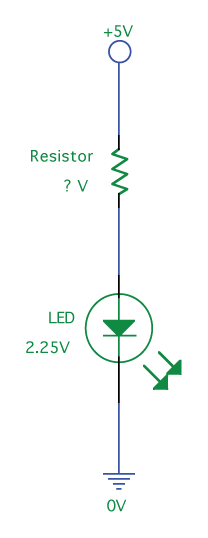 Figure 3.9 LED Circuit |
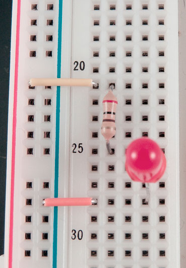 Figure 3.10 Wired LED |
LED Polarity An LED typically has two leads projecting from its base (Figure 3.11). The longer of the two is the positive lead (also known as the "anode"), and the shorter, the negative lead (also known as the "cathode"). The cathode is also denoted by a flat edge on the plastic LED housing. The anode will connect to positive voltage (5V in this case) and the cathode will connect to ground.
Resistor Codes Most resistors have four colored bars, which will give you the value in Ohms, as shown in Table 3.1. A resistor of yellow-red-red-gold would be 4,200 Ohms, with an accuracy of 5%. If we needed a 30-Ohm resistor, we would search for with the colors orange-black-brown-gold. Memorizing this chart will save you time if you're going to do a lot of work with resistors. At the very least, knowing the values in column three will help prevent you from using an exponentially incorrect resistor. If you don't have the time to memorize them or have no desire to haul the chart around with you, there are a multitude of Java applets on the Internet which will do the conversions for you. There are also many applications for graphing calculators that allow you to complete the conversion without the work. These include RCOL for the HP 48, which is available at hpcalc.org. Finally, you can also use your multimeter to measure the resistance. |
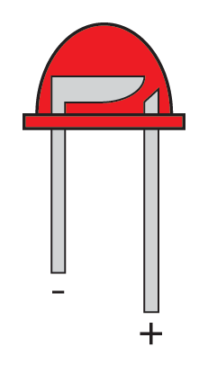
Table 3.1 Resistor Codes
Color
Bar 1
Bar 2
Bar 3
Bar 4
Black
0
0
x1
Brown
1
1
x10
Red
2
2
x100
Orange
3
3
x1,000
Yellow
4
4
x10,000
Green
5
5
x100,000
Blue
6
6
x1,000,0000
Magenta
7
7
Gray
8
8
White
9
9
Gold
x0.1
5%
Silver
x0.01
10%
Capacitors
A capacitor (Figure 3.12) stores energy in an electric field. In building our circuits, we'll be using these as de-spiking capacitors to filter the power supply. When the output of one of our chips changes, it causes a sudden voltage drop (a negative-going spike). When this occurs, the capacitor will partially discharge its energy to reduce the severity of this spike.

Figure 3.12 Capacitors
Gates
Those little black chips that cover circuit boards look extremely complex. Today, most of these integrated circuits (ICs) are quite intricate, but there are still many simpler chips available. If you examine the chips in a modern computer, you will notice that many of them have hundreds of pins, placed so closely that they appear almost impossible to work with. Open an older computer, and you'll discover chips that look much more accessible, with few pins and wider spacing. These older, more "classic" chips are what we'll be working with through the duration of this book. The 7400 series of ICs serves as the basis for digital logic and is very easy to understand. Throughout the rest of this chapter we'll concentrate on building a few very basic digital circuits using 7400-series ICs, resistors, and LEDs.
AND
IF it is dark AND IF there is a car in the driveway THEN turn on the porch light.
Under what circumstances is the porch light turned on? Only if both statements are true—it must be dark and there must be a car in the driveway. One of the two is not enough. In a schematic, we'd express this as seen in Figure 3.13. The "D" symbol is a logical AND. We can also use a truth table. Follow along with the truth tables in Table 3.2 and see if they match the aforementioned assertions. You'll note that all three tables contain the same data. True is a logical "1" which is implemented with a 5-volt signal. False is a logical "0" and is implemented by a 0-volt signal.
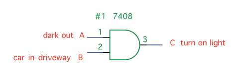
Figure 3.13 AND Gate
| Input A | Input B | Output C |
| False | False | False |
| False | True | False |
| True | False | False |
| True | True | True |
| Input A | Input B | Output C |
| 0 | 0 | 0 |
| 0 | 1 | 0 |
| 1 | 0 | 0 |
| 1 | 1 | 1 |
| Input A | Input B | Output C |
| 0V | 0V | 0V |
| 0V | 5V | 0V |
| 5V | 0V | 0V |
| 5V | 5V | 5V |
With all of this in mind, perform the following steps:
- Take a 7408 IC and insert it into your breadboard. This chip has four AND gates, arranged as shown in Figure 3.14. Note the location of the notch in the diagram.
- Orient all chips so that the notch is at the top, and pin 1 will always be in the upper-left corner.
- Hook up the supply voltage and ground. Pin 14 is Vcc (Voltage common collector) and should be tied to your 5-volt line. Pin 7, GND, should be connected to ground.
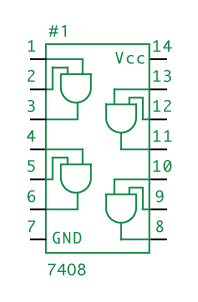
Figure 3.14 7408 IC
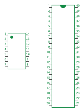
Pin Numbering Pin numbering always starts at the upper-left corner, goes down the left side, and follows up the right side. Pin 1 is marked either by a circle in the upper-left corner, or by a notch in the top center (at which point it's up to you to know left from right). See Figure 3.15:
|
Now let's wire the first AND gate on the chip:
- Connect pins 1 and 2 (inputs to the AND gate) to the supply voltage line.
- Connect pin 3 to the input of the LED that was wired up in Figure 3.10.
- Turn on the power, wait a few nanoseconds for the signal to propagate, and the LED should light up (Figure 3.16). Since both Input A and Input B are high, the output will also be high and the LED will be powered on.
- Take the wire from pin 2 (or pin 1) and move it from supply voltage to ground. To grasp the importance of this, imagine that instead of moving the cable by hand, it's hooked up to a light sensor that outputs 0 volts when it's bright outside, and 5 volts when it's dark.
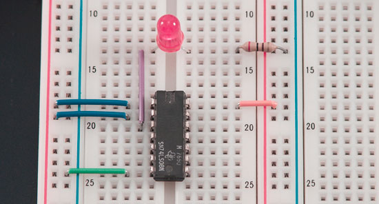
Figure 3.16 Using AND With an LED
Nanoseconds When a chip's inputs are changed, the output does not change instantaneously. The new signals take time to propagate throughout the chip. This propagation varies depending upon the speed and complexity of the design, but TTL gates tend to take about 10 nanoseconds (ns) to complete propagation. There are 1,000,000,000 nanoseconds in a second. |
If you like a challenge, try playing around with the chip a bit more by wiring the inputs of some gates up to the outputs of others. Create the equivalent of a 4-input AND gate. You can also examine the logic table in Table 3.3 to find patterns.
| Input A | Input B | Input C | Input D | Output E |
| 0 | 0 | 0 | 0 | 0 |
| 0 | 0 | 0 | 1 | 0 |
| 0 | 0 | 1 | 0 | 0 |
| 0 | 0 | 1 | 1 | 0 |
| 0 | 1 | 0 | 0 | 0 |
| 0 | 1 | 0 | 1 | 0 |
| 0 | 1 | 1 | 0 | 0 |
| 0 | 1 | 1 | 1 | 0 |
| 1 | 0 | 0 | 0 | 0 |
| 1 | 0 | 0 | 1 | 0 |
| 1 | 0 | 1 | 0 | 0 |
| 1 | 0 | 1 | 1 | 0 |
| 1 | 1 | 0 | 0 | 0 |
| 1 | 1 | 0 | 1 | 0 |
| 1 | 1 | 1 | 0 | 0 |
| 1 | 1 | 1 | 1 | 1 |
Inverter, NAND
IF it is dark AND IF there is a car in the driveway THEN turn OFF the porch light.
This statement is almost identical to the one in the previous section, even though our goal has changed to producing the opposite effect. The only change that needs to be made is the addition of an inverter (see Table 3.4). The inverter takes whatever signal it is given and outputs the opposite; if you put 0 volts in, you'll get 5 volts out, and vice versa. In Figure 3.17, you'll see the symbol for an inverter along with an AND gate. The triangle means "buffer" (replicate the signal) and the small circle means "invert it." Find a 7404 (Figure 3.18) and connect it to supply voltage and ground. Now connect the output of your AND gate (pin 3) to the input of the 7404's inverter (pin 1). The output of the inverter (pin 2) goes to the LED to complete our circuit, shown in Figure 3.19.
| Input A | Output B |
| 0 | 1 |
| 1 | 0 |
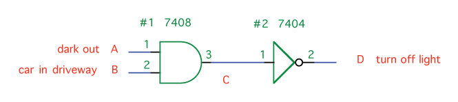
Figure 3.17 7404 IC
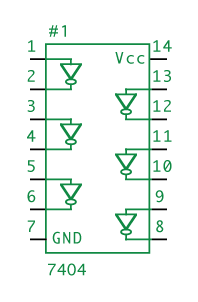
Figure 3.18 AND Inverted
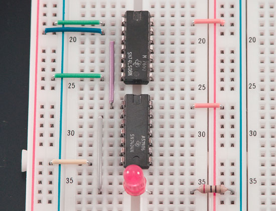
Figure 3.19 AND and NAND Gates, Wired to LED
The inverted AND is so common that it has its own gate, the NAND (Not AND) gate. This gate is functionally equivalent to an AND followed by an inverter. The NAND is pictured in Figure 3.20, with its layout in Figure 3.21. Table 3.5 displays its operation, which, hopefully, you were able to surmise.
| Input A | Input B | Output C |
| 0 | 0 | 1 |
| 0 | 1 | 1 |
| 1 | 0 | 1 |
| 1 | 1 | 0 |
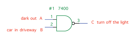
Figure 3.20 NAND Gate
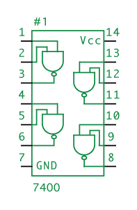
Figure 3.21 7400 IC
OR, NOR
IF it is dark AND IF there is a car in the driveway OR if the light switch is on THEN turn on the porch light.
Here we take our output from the AND gate and OR it with "the light switch is on." The OR gate in TTL logic is the 7432 (Figure 3.22), and exhibits the characteristics provided in Table 3.6.
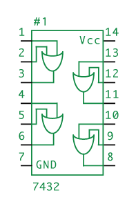
Figure 3.22 7432 IC
| Input A | Input B | Output C (A OR B) |
| 0 | 0 | 0 |
| 0 | 1 | 1 |
| 1 | 0 | 1 |
| 1 | 1 | 1 |
Perform the following steps:
- Take your 7432 and connect power and ground.
- Using the circuit from Figure 3.16, hook the output of the AND gate to an input of the OR (pin 1). The other OR input (pin 2) should be connected directly to power or ground to simulate the light switch being on or off.
- Next, wire the OR's output (pin 3) to the LED (Figure 3.23). Table 3.7 describes the behavior of this entire circuit. Note that the light comes on for five out of the eight possible combinations.
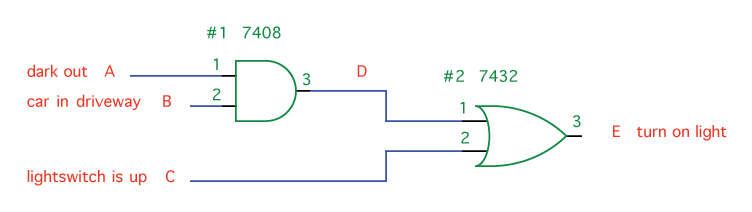
Figure 3.23 AND and OR, Wired
| Input A | Input B | A AND B | Input C | Output E ((A AND B) OR C) |
| 0 | 0 | 0 | 0 | 0 |
| 0 | 1 | 0 | 0 | 0 |
| 1 | 0 | 0 | 0 | 0 |
| 1 | 1 | 1 | 0 | 1 |
| 0 | 0 | 0 | 1 | 1 |
| 0 | 1 | 0 | 1 | 1 |
| 1 | 0 | 0 | 1 | 1 |
| 1 | 1 | 1 | 1 | 1 |
Like NAND, there is also a NOR gate (Figure 3.24), which is OR followed by an inverter. You can find NOR gates on the 7402 (Figure 3.25).
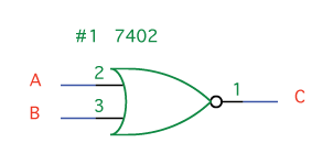
Figure 3.24 NOR Gate
| Input A | Input B | Output C (A NOR B) |
| 0 | 0 | 1 |
| 0 | 1 | 0 |
| 1 | 0 | 0 |
| 1 | 1 | 0 |
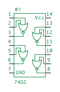
Figure 3.25 7402 IC
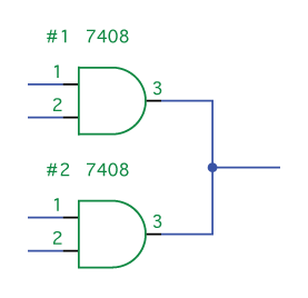
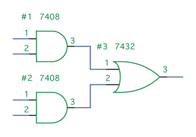
Combining Outputs with OR Let's say you have two AND gates and you want to combine their outputs so that if either AND gate's output is HI, our final output is HI as well. What happens if you connect the two output lines, as in Figure 3.26? When output A goes HI and output B goes LO, the two signals will compete, potentially damaging your chips. If you're tempted to try this configuration, you're probably looking to use an OR gate, as in Figure 3.27.
|
XOR
IF it is dark OR IF there is a car in the driveway—but NOT if both—THEN turn on the porch light.
Perhaps this behavior would be desirable if you wanted to discourage visitors after dusk. XOR is short for "exclusive OR" and means "if one or the other is true, but not if both are true." You can find XOR gates on the 7486 (Figure 3.28). In Figure 3.29 is the schematic for this circuit, along with an equivalent circuit that does not use an XOR gate but achieves the same effect.
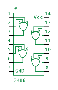
Figure 3.28 7486 IC
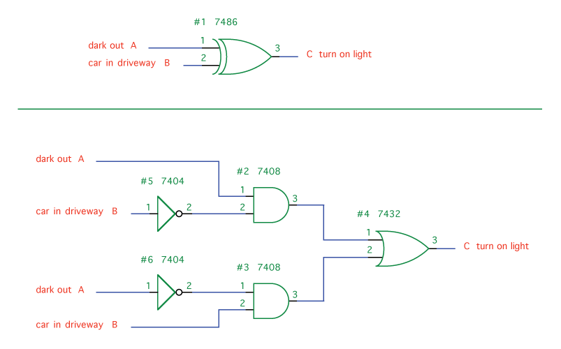
Figure 3.29 XOR Gate Circuit
| Input A | Input B | Output C (A XOR B) |
| 0 | 0 | 0 |
| 0 | 1 | 1 |
| 1 | 0 | 1 |
| 1 | 1 | 0 |
Circuits with Algebra
Don't worry, it's not as bad as it sounds. Using logic expressions, DeMorgan's Laws, and Boolean algebra, you can quickly sketch out basic circuits on paper or even in a simple text editor. Logic expressions will allow you to show gates and lines with symbols and letters. DeMorgan's Laws will allow you to swap gates in order to get more efficient circuits. Boolean algebra will allow you to simplify your circuits.
Logic Expressions
Ambiguities in the English language can make it very difficult to precisely express digital logic, so a specific algebra has been developed for this purpose. Understanding this algebra is merely a matter of getting accustomed to its symbols. Table 3.10 displays these symbols, listed in order of precedence:
| Symbol | Meaning |
| ' | NOT |
| • | AND |
| + | OR |
| ⊕ | XOR |
Figure 3.30 shows a few logic expressions and their equivalent circuits. Take a good look at these and make sure you understand them. Try writing a few of your own.
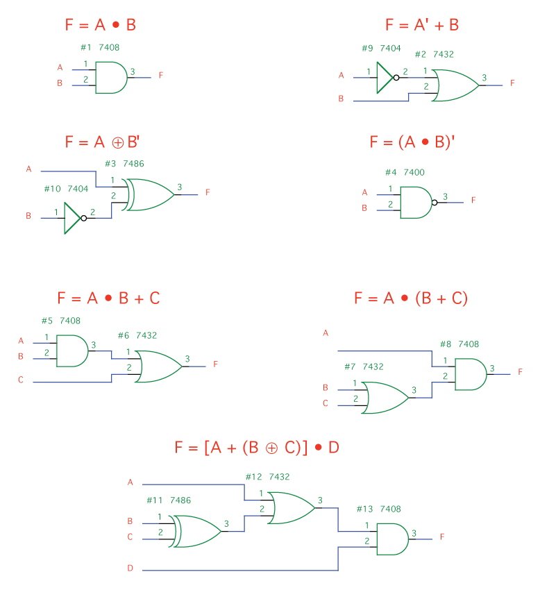
Figure 3.30 Equivalent Circuits for Logic Expressions
DeMorgan's Laws
DeMorgan's Laws sounds dull and tedious, but they're a real boon for the improvising hacker. These laws explain how we can substitute different combinations of gates to best use our available resources. They can be expressed as:
(A + B) ' = A' • B'
(A • B) ' = A' + B'
Let's take (A • B) ' for example (a NAND gate). This statement means that A and B are not both true; therefore, at least one of them is false. Consequently, it follows that A is not true or B is not true, which we can write as A' + B'. This looks like a slight change, but it can make a huge difference. Consider, for example, that the signals you are receiving may already be inverted or that you may not even have any NAND gates. Also, note that each of the chips we've been using contains multiple gates. DeMorgan's Laws allow us to more fully utilize the chips with which we're already working.
There's an easy way to remember DeMorgan's Laws in practice (Figure 3.31). To find the equivalent for any gate, first swap its symbol (OR to AND, AND to OR). Then, look at each input and output. Everywhere there's an inverter, remove it, and everywhere there isn't, add one.
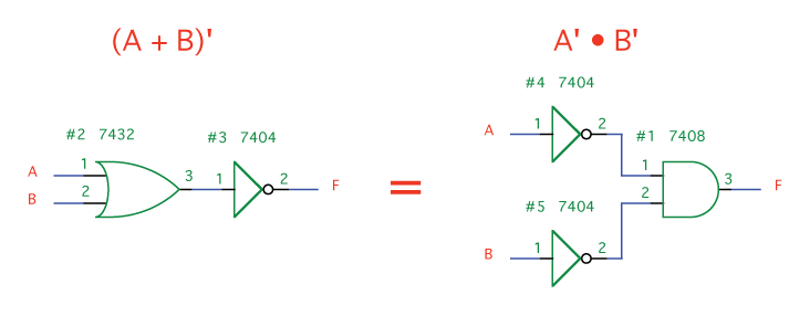
Figure 3.31 DeMorgan's Laws
Boolean Algebra
Boolean algebra is a method for manipulating logic expressions. It allows us to take complex expressions and reduce them to simpler statements that are logically equivalent. Some useful equivalencies are shown in Table 3.11.
| A • 1 = A | A + 0 = A |
| A • 0 = 0 | A + 1 = 1 |
| A •A = A | A + A = A |
| A •A' = 0 | A + A' = 1 |
| (A') ' = A | ((A') ') ' = A' |
| A • B + A • C = A • (B + C) | (A + B) • (A + C) = A + (B • C) |
| A • (A + B) = A | A + (A • B) = A |
| A • (A' + B) = A •B | A + (A' • B) = A + B |
| (A •B) ' = A' + B' | (A + B) ' = A' • B |
Make sure you understand why all of these equivalences are true. Let's take
A + 1 = 1
as an example. The statement reads "if A is 1 or if 1 is 1." Given that "1" is always "1," this statement is always true and we can simply assert "1."
All You Need is NAND
We've already shown that XOR can be expressed as a combination of AND and OR gates (Figure 3.29). Likewise, NAND and NOR can be expressed by using an inverter along with AND and OR, respectively. Thanks to DeMorgan's Laws, we can use a combination of inverters and OR gates to produce an AND gate, or a combination of inverters and AND gates to produce an OR gate. At this point, we have a means of re-expressing every gate except the inverter. We can do that with a NAND gate. Connect both inputs of your NAND gate to the same line (we'll call it P). A NAND gate is expressed:
(A • B) ' = C
Since in our case, both A and B are the same line, we can write:
(P • P) ' = C
Using the equivalence
A • A = A
given in the previous section, we can reduce this to
(P) ' = C
which means that our NAND gate now functions as an inverter.
A complete set is a collection of chips that can be used to produce any logical statement. One example of a complete set would be the 7408 (AND), 7432 (OR), and the 7404 (NOT). Another example is the 7400 (NAND). Any circuit can be built by using nothing but NAND. This means that any computer of any complexity could be built using only 7400 ICs. This is not practical when you consider the colossal size such a computer would have to be, but it is interesting to consider the magnitude of the concepts you can express using nothing but NAND.
A second NAND gate is used to negate the negation, and we're back to an ordinary AND (Figure 3.32).
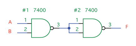
Figure 3.32 AND with NANDs
Thanks to DeMorgan's Laws, we know that an AND gate surrounded by inverters is equivalent to an OR (Figure 3.33).
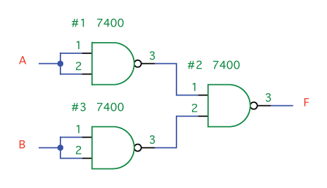
Figure 3.33 OR with NANDs
An XOR gate can be expressed as (A • B') + (A' • B). Using that equivalency and the previous examples as parts, we can express an XOR using nine NAND gates (Figure 3.34). This circuit, incidentally, can be reduced to five NAND gates pretty easily and there's also a way to do it with just four.
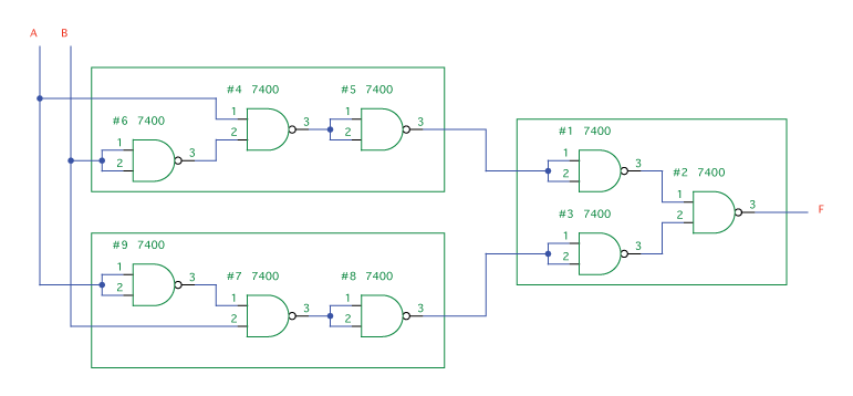
Figure 3.34 XOR with NANDs
Latches and Flip-Flops
You may have noticed a shortcoming in the circuits we've described thus far. What if we want the porch light to stay on after it detects a car in the driveway? The circuits we've covered have no memory. Now we're going to discuss ways of adding memory to our circuits, using only the gates we've covered in previous sections.
SR Latch
A set-reset (SR) latch allows us to "set" a bit to 1 or "reset" it to 0. We can do this using ordinary logic gates. The trick is to loop the output back into the input (Figure 3.35).
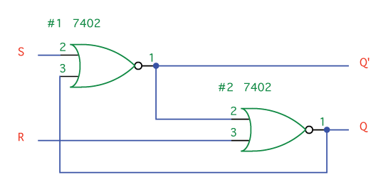
Figure 3.35 SR Latch
Grab a 7402 and wire up this circuit. Connect an LED to the output Q (Figure 3.36).
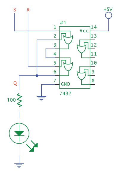
Figure 3.36 TTL SR Latch
This circuit is confusing because our outputs are determining our inputs. Consequently, the first thing we need to do when we power this circuit on is to "reset" it, so that we have a circuit with known outputs. Looking at the #2 NOR gate, we can see that the input R alone being high is enough to make the output Q low. In your circuit, wire R to high and S to low. The output Q will be low. Now, check the inputs to the #1 NOR gate. Both of these are low, making Q' high. Q' is an input to the lower NOR gate. This means that even when Reset goes low, the circuit will stay in the reset state.
Now, let's take R low and make S high. The output of the #1 NOR becomes 0, which means both inputs to the #2 NOR are now 0, making the Q output 1. Make S low and Q stays high, because Q is being looped back into the input of the #1 NOR gate. Q will remain high until the circuit is reset.
Table 3.12 is the complete table of operation. What's most important to realize here is that all it takes is a momentary high on the set or reset lines to permanently set or reset the output Q.
| S | R | Q |
| 0 | 0 | Previous value of Q |
| 0 | 1 | 0 |
| 1 | 0 | 1 |
| 1 | 1 | Not used |
Flip-Flop
Imagine we have a situation where we want to grab a value at a certain instant and then hold onto it. For example, "every hour, check to see if the water level is above the indicator. If it is, sound the alarm for a full hour, then check again." We can accomplish this using a D flip-flop.
Figure 3.37 shows the circuit in order to help you build it on your breadboard. We're not going to examine its operation, but if you want to figure it out, follow the levels in your mind or with a logic probe. Normally, when you see a flip-flop in a schematic, it'll look like Figure 3.38.
If you don't want to wire up all those NAND gates, use a 7474 TTL flip-flop, which is shown in Figure 3.39. Notice the inverters at the inputs to the Preset and Clear lines. Due to their presence, we use a HI signal instead of a LO to deactivate these lines.
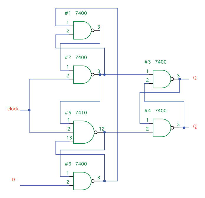
Figure 3.37 Flip-Flop in Logic Gates
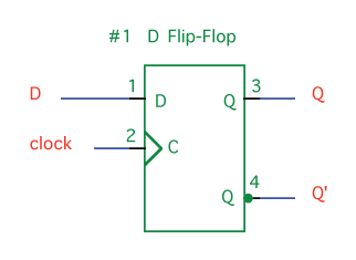
Figure 3.38 D Flip-Flop
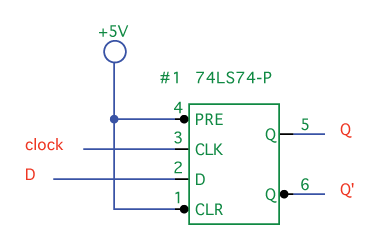
Figure 3.39 74LS74 IC
To use the circuit, perform the following steps:
- Connect the clock input to LO and the D input to whatever value you want (let's say 1, in this case).
- Now we want to pulse the clock. Disconnect the clock from LO, touch it to HI, then move it back to LO. That's a pulse. In a D flip-flop, a pulse is detected at the moment of the change from LO to HI.
- You can leave the clock connected to HI for as long as you like and it is still only seen as a single pulse.
What is Data?
Before we look at the more complex chips that are used in the Apple I, we need to understand what all this data is that we're passing around.
Counting in Binary and Hexadecimal
Digital logic only has two states, high or low; so, our numbers need to be expressed in binary (base-2) format. A binary digit, like a digital signal, is always either 1 or 0. Converting from decimal to binary is tedious, but you can calculate the values quickly by adding up each place value.
Consider in decimal we have place values 1, 10, 100, etc., such that we could calculate the number 203 by multiplying the digit by the place value:
(2 x 100) + (0 x 10) + (3 x 1) = 203
In binary we can do the same thing, except that our place values are now 1, 2, 4, 8, and so on (see Table 3.13). If we take 1101, we can calculate:
(1 x 8) + (1 x 4) + (0 x 2) + (1 x 1) = 13
| Decimal | Binary | Hexadecimal |
| 1,000,000 | 64 | 16,777,216 |
| 100,000 | 32 | 1,048,576 |
| 10,000 | 16 | 65,536 |
| 1,000 | 8 | 4,096 |
| 100 | 4 | 256 |
| 10 | 2 | 16 |
| 1 | 1 | 1 |
Distinguishing Numbers If we write "10," is it a decimal "10" or a binary "two?" To distinguish binary numbers from decimal numbers, append a 'b' to the end so that it reads "10b." Hexadecimal numbers are prefixed with a '$' or sometimes with "0x;" hence, a hexadecimal "10" would look like "$10" or "0x10." |
Each digit in binary is called a bit. With 10 bits, we can express 0 through 1023 in binary. Note that you also have 10 fingers. Counting on your fingers, with each finger corresponding to a bit, is a good way to get used to the binary system (Figure 3.40). As you count, you'll also notice some patterns, which are also apparent in Table 3.14. The ones column alternates 0 and 1 with each row; the tens column alternates every two rows, and so on.

Figure 3.40 125 in Binary
| Decimal | Binary | Exponential | Hexadecimal |
| 0 | 0000 0000b | 0 | $00 |
| 1 | 0000 0001b | 20 | $01 |
| 2 | 0000 0010b | 21 | $02 |
| 3 | 0000 0011b | 21 + 20 | $03 |
| 4 | 0000 0100b | 22 | $04 |
| 5 | 0000 0101b | 22 + 20 | $05 |
| 6 | 0000 0110b | 22 + 21 | $06 |
| 7 | 0000 0111b | 22 + 21 + 20 | $07 |
| 8 | 0000 1000b | 23 | $08 |
| 9 | 0000 1001b | 23 + 20 | $09 |
| 10 | 0000 1010b | 23 + 21 | $0A |
| 11 | 0000 1011b | 23 + 21 + 20 | $0B |
| 12 | 0000 1100b | 23 + 22 | $0C |
| 13 | 0000 1101b | 23 + 22 + 20 | $0D |
| 14 | 0000 1110b | 23 + 22 + 21 | $0E |
| 15 | 0000 1111b | 23 + 22 + 21 + 20 | $0F |
| 16 | 0001 0000b | 24 | $10 |
| 17 | 0001 0001b | 24 + 20 | $11 |
| 18 | 0001 0010b | 24 + 21 | $12 |
| 19 | 0001 0011b | 24 + 21 + 20 | $13 |
| 20 | 0001 0100b | 24 + 22 | $14 |
| ... | ... | ... | ... |
| 32 | 0010 0000b | $20 | |
| 64 | 0100 0000b | $40 | |
| 128 | 1000 0000b | $80 | |
| 255 | 1111 1111b | $FF | |
| 256 | 0000 0001 0000 0000b | $01 00 | |
| 1000 | 0000 0011 1110 1000b | $03 E8 | |
| 1023 | 0000 0011 1111 1111b | $03 FF | |
| 1024 | 0000 0100 0000 0000b | $04 00 | |
| 14287 | 0011 0111 1100 1111b | $37 CF | |
| 65535 | 1111 1111 1111 1111b | $FF FF |
Binary numbers are difficult to read and write, not to mention pronounce. Fortunately, they're very easy to translate into the more convenient hexadecimal format (base-16). Note that the binary numbers in the table are divided into groups of four. With four bits, we can count up to 15, which correlates perfectly with hexadecimal. Since we only have 10 symbols (0-9) in decimal, we need to create six more for hexadecimal. For these last six symbols, the letters A through F are used. For example, 'B' is 11, 'C' is 12, and 'F' is 15. Let's take a look at a few hexadecimal examples using place-value calculations.
$CF = (12 x 16) + (15 x 1) = 207
$10 = (1 x 16) + (0 x 1) = 16
$FFFF = (15 x 4096) + (15 x 256) + (15 x 16) + (15 x 1) = 65535
Bytes
There's not much that can be expressed with a single bit, so computers examine a collection of bits at one time. This collection of bits is called a word. Modern computers have 32 or 64-bit words. Traditionally, personal computers such as the Apple I have used an 8-bit word, which is why you'll often hear computers from the 1970s and early '80s referred to as "8-bit microcomputers." This 8-bit word is known as a byte.
Eight bits can be used to represent any letter in the alphabet, a computer instruction, a number, the color of a pixel, or data in countless other formats. A byte is not significantly harder to work with than a single bit. An 8-bit flip-flop (called a register), for example, is just eight flip-flops connected to the same clock (Figure 3.41).
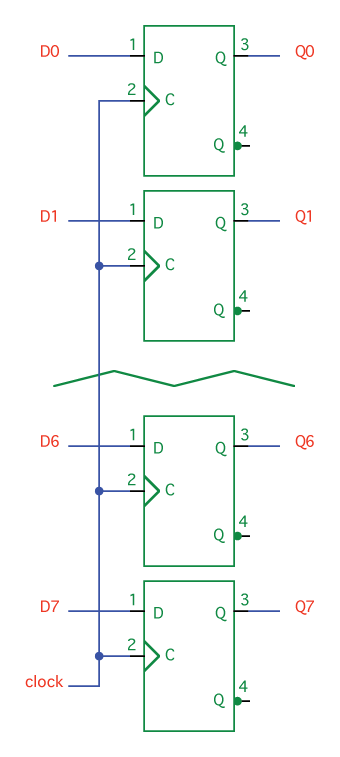
Figure 3.41 Flip-Flops in Parallel
When we work with eight bits, it can become very repetitive drawing identical objects one after the other, eight times. A shortcut is therefore adopted where we use a single (usually thicker) line to represent multiple lines. The circuit in Figure 3.42 is equivalent to that in Figure 3.41, but it takes less space and is quicker to read. If you're using schematic software such as McCAD, it may forgo the slash and merely use a thicker line.
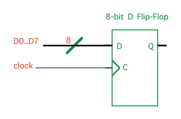
Figure 3.42 8-Bit D Flip-Flop
A selection of lines (such as D0 through D7) treated as a group is called a bus. Since our Apple I circuit is based on bytes, we will be using an 8-bit bus quite extensively. A bus can be either parallel or serial. If you're familiar with the parallel and serial ports used on PCs and the Apple II, you probably already have an idea of the difference between the two. In a parallel bus, which we've seen in Figures 3.41 and 3.42, every bit is on its own line and arrives at the same time. Every clock pulse, a new byte of data arrives. This bus is the simplest to use and to understand.
The other option, a serial bus, uses a single data line. All data arrives over this single line, one bit after the next. Each time the clock pulses, the next bit arrives and must be saved by the receiving device. Once the eighth bit arrives, the recipient can examine the entire byte. Upon the next clock pulse, the first bit of the next byte arrives.
Nibbles and Bits A nibble is four bits—half a byte (get it?). The term is not often used, but is mentioned here for completeness. |
ASCII and the Alphabet
A byte has 256 possible combinations, more than enough to represent the entire alphabet. The American National Standards Institute (ANSI) developed a standardized code in the 1960s to facilitate the exchange of information between different computers. Called the American Standard Code for Information Interchange (ASCII), it remains in common use today. ASCII uses seven bits to produce the 128 characters enumerated in Table 3.15.
| Dec | Hex | Char | Dec | Hex | Char | Dec | Hex | Char | Dec | Hex | Char | |||
| 0 | 0 | NUL (null) | 32 | 20 | Space | 64 | 40 | @ | 96 | 60 | ` | |||
| 1 | 1 | SOH (start of heading) | 33 | 21 | ! | 65 | 41 | A | 97 | 61 | a | |||
| 2 | 2 | STX (start of text) | 34 | 22 | " | 66 | 42 | B | 98 | 62 | b | |||
| 3 | 3 | ETX (end of text) | 35 | 23 | # | 67 | 43 | C | 99 | 63 | c | |||
| 4 | 4 | EOT (end of transmission) | 36 | 24 | $ | 68 | 44 | D | 100 | 64 | d | |||
| 5 | 5 | ENQ (enquiry) | 37 | 25 | % | 69 | 45 | E | 101 | 65 | e | |||
| 6 | 6 | ACK (acknowledge) | 38 | 26 | & | 70 | 46 | F | 102 | 66 | f | |||
| 7 | 7 | BEL (bell) | 39 | 27 | ' | 71 | 47 | G | 103 | 67 | g | |||
| 8 | 8 | BS (backspace) | 40 | 28 | ( | 72 | 48 | H | 104 | 68 | h | |||
| 9 | 9 | TAB (horizontal tab) | 41 | 29 | ) | 73 | 49 | I | 105 | 69 | i | |||
| 10 | A | LF (line feed) | 42 | 2A | * | 74 | 4A | J | 106 | 6A | j | |||
| 11 | B | VT (vertical tab) | 43 | 2B | + | 75 | 4B | K | 107 | 6B | k | |||
| 12 | C | FF (form feed) | 44 | 2C | , | 76 | 4C | L | 108 | 6C | l | |||
| 13 | D | CR (carriage return) | 45 | 2D | - | 77 | 4D | M | 109 | 6D | m | |||
| 14 | E | SO (shift out) | 46 | 2E | . | 78 | 4E | N | 110 | 6E | n | |||
| 15 | F | SI (shift in) | 47 | 2F | / | 79 | 4F | O | 111 | 6F | o | |||
| 16 | 10 | DLE (data link escape) | 48 | 30 | 0 | 80 | 50 | P | 112 | 70 | p | |||
| 17 | 11 | DC1 (device control 1) | 49 | 31 | 1 | 81 | 51 | Q | 113 | 71 | q | |||
| 18 | 12 | DC2 (device control 2) | 50 | 32 | 2 | 82 | 52 | R | 114 | 72 | q | |||
| 19 | 13 | DC3 (device control 3) | 51 | 33 | 3 | 83 | 53 | S | 115 | 73 | s | |||
| 20 | 14 | DC4 (device control 4) | 52 | 34 | 4 | 84 | 54 | T | 116 | 74 | t | |||
| 21 | 15 | NAK (neg. acknowledge) | 53 | 35 | 5 | 85 | 55 | U | 117 | 75 | u | |||
| 22 | 16 | SYN (synchronous idle) | 54 | 36 | 6 | 86 | 56 | V | 118 | 76 | v | |||
| 23 | 17 | ETB (end of trans.) | 55 | 37 | 7 | 87 | 57 | W | 119 | 77 | w | |||
| 24 | 18 | CAN (cancel) | 56 | 38 | 8 | 88 | 58 | X | 120 | 78 | x | |||
| 25 | 19 | EM (end of medium) | 57 | 39 | 9 | 89 | 59 | Y | 121 | 79 | y | |||
| 26 | 1A | SUB (substitute) | 58 | 3A | : | 90 | 5A | Z | 122 | 7A | z | |||
| 27 | 1B | ESC (escape) | 59 | 3B | ; | 91 | 5B | [ | 123 | 7B | { | |||
| 28 | 1C | FS (file separator) | 60 | 3C | < | 92 | 5C | \ | 124 | 7C | | | |||
| 29 | 1D | GS (group separator) | 61 | 3D | = | 93 | 5D | ] | 125 | 7D | } | |||
| 30 | 1E | RS (record separator) | 62 | 3E | > | 94 | 5E | ^ | 126 | 7E | ~ | |||
| 31 | 1F | US (unit separator) | 63 | 3F | ? | 95 | 5F | _ | 127 | 7F | DEL |
A Few More Chips
Shift Register
A shift register is a collection of flip-flops hooked up in a row such that the output of one is the input to the next (Figure 3.43). This allows us to store a series of data as it comes in—one bit every clock pulse. Let's assume that at every pulse of the clock, a new bit of data arrives on the input line, which is, in fact, usually the case. This data will be:
101100000...
Though most shift registers have a "clear" input to reset all the flip-flops to 0, ours does not. Therefore, we're going to assume that the content of the flip-flops before we enter our data is unknown (either 0 or 1). This will be represented in our table by an "x." We also use "t" to represent time. For example, t0 is when we begin, t1 is immediately after the first clock pulse, t2 after the second pulse, and so on.

Figure 3.43 Shift Register with D Flip-Flops
At t0 we don't know the contents of any of the flip-flops, but some time before the first clock pulse, a 1 arrives on the D input line. At t1, the clock pulses, and this 1 is loaded into the first flop-flop. As soon as it is loaded into that flip-flop, it becomes present on the Q output. At t2, the clock pulses again. At this instant, 1 is loaded into flip-flop #2 and the next 0 is loaded into flip-flop #1. You can see the full continuation of this process in Table 3.16.
| t0 | t1 | t2 | t3 | t4 | t5 | t6 | t7 | t8 | t9 | |
| FF #1 | x | 1 | 0 | 1 | 1 | 0 | 0 | 0 | 0 | 0 |
| FF #2 | x | x | 1 | 0 | 1 | 1 | 0 | 0 | 0 | 0 |
| FF #3 | x | x | x | 1 | 0 | 1 | 1 | 0 | 0 | 0 |
| FF #4 | x | x | x | x | 1 | 0 | 1 | 1 | 0 | 0 |
Buffer and Tri-State Buffer
There are occasions when we want to use the output of one gate as the input to quite a few other gates, but we're limited by the fact that a TTL gate can only drive 10 other gates. To alleviate this problem, we have buffers. As you can see in Table 3.17, a buffer is like an inverter that doesn't invert—it just takes the signal and replicates it. Each buffer we have on an output can drive 10 more gates.
| Input A | Output Y |
| 0 | 0 |
| 1 | 1 |
A tri-state buffer is even more interesting. When we discussed OR gates, we looked at how a gate's output is either low or high, 0 or 1. Tri-state buffers add a third state—off. In this third state, "floating," no output at all comes from the chip and it will not interfere with other signals on the line.
Examine Figure 3.44 and Table 3.18. You can think of line G as a valve that turns on the flow of electricity. As long as G is low (i.e. the flow is turned off), you can put any signal you want on the output lines without harming the chip. This allows us to create circuits such as the one in Figure 3.45. Beware, though—if both gates' outputs are turned on at the same time, you'll damage your chips. If you'd like to try wiring some of these up yourself, you can use the 74LS367 (Figure 3.46).
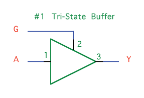 Figure 3.44 Tri-State Buffer |
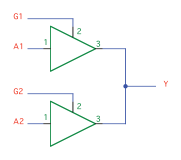 Figure 3.45 Circuit with Tri-State Buffers |
| Input A | Input G | Output Y |
| 0 | 0 | x |
| 0 | 1 | 0 |
| 1 | 0 | x |
| 1 | 1 | 1 |
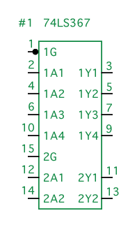
Figure 3.46 74LS367 IC
Encoders and Decoders
We have eight inputs. Line six is high. Let's say we want to send the number 6 to our computer, or to some output device such as a numeric display. The receiving device is going to expect this data in binary format. If you've paid attention to the patterns in binary digits, a binary encoder is not very difficult to make. To express numbers between 0 and 7 in binary, we need three bits. Examine the patterns in Table 3.14 and you'll see that the lowest bit (bit 0) alternates between 0 and 1, such that bit 0 is high for 1, 3, 5, and 7. The second lowest bit (bit 1) alternates every two lines between 0 and 1, so it's high for 2, 3, 6, and 7. Finally, bit 3 alternates every four lines, so it's high for 4, 5, 6, and 7. This circuit is expressed in Figure 3.47. The same circuit is shown in Figure 3.48 as an ordinary encoder.
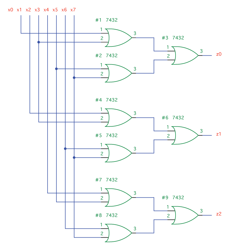
Figure 3.47 Encoder with Gates
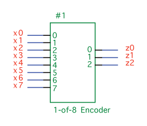
Figure 3.48 1-of-8 Encoder
Is it possible to go in the reverse from binary to single-line output? Let's design a 1-of-8 decoder (Figure 3.49). First, fill out a truth table (Table 3.19). Consider writing this out by hand before looking ahead. Remember that your inputs (x0, x1, x2) represent the binary digits and z0 through z7 are your outputs, so when you're filling out the table, fill in all the inputs before solving the outputs, line by line.
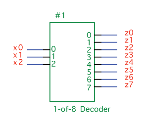
Figure 3.49 1-of-8 Decoder
| x2 | x1 | x0 | z0 | z1 | z2 | z3 | z4 | z5 | z6 | z7 | |
| 0 | 0 | 0 | 1 | 0 | 0 | 0 | 0 | 0 | 0 | 0 | |
| 0 | 0 | 1 | 0 | 1 | 0 | 0 | 0 | 0 | 0 | 0 | |
| 0 | 1 | 0 | 0 | 0 | 1 | 0 | 0 | 0 | 0 | 0 | |
| 0 | 1 | 1 | 0 | 0 | 0 | 1 | 0 | 0 | 0 | 0 | |
| 1 | 0 | 0 | 0 | 0 | 0 | 0 | 1 | 0 | 0 | 0 | |
| 1 | 0 | 1 | 0 | 0 | 0 | 0 | 0 | 1 | 0 | 0 | |
| 1 | 1 | 0 | 0 | 0 | 0 | 0 | 0 | 0 | 1 | 0 | |
| 1 | 1 | 1 | 0 | 0 | 0 | 0 | 0 | 0 | 0 | 1 |
Next, write logic statements based on this truth table. For example, z0 is high only when x2 is not high, x1 is not high, and x0 is not high; hence, we write: z0 = x0' • x1' • x2'. The complete set of logic statements is:
z0 = x0' • x1' • x2'
z1 = x0 • x1' • x2'
z2 = x0' • x1 • x2'
z3 = x0 • x1 • x2'
z4 = x0' • x1' • x2
z5 = x0 • x1' • x2
z6 = x0' • x1 • x2
z7 = x0 • x1 • x2
Finally, we draw a circuit based on these logic gates (Figure 3.50). (You might notice that this circuit uses three more inverters than it needs to. There are two ways to cut the number of inverters in half, by using DeMorgan's Laws or by simply rearranging some wires.)
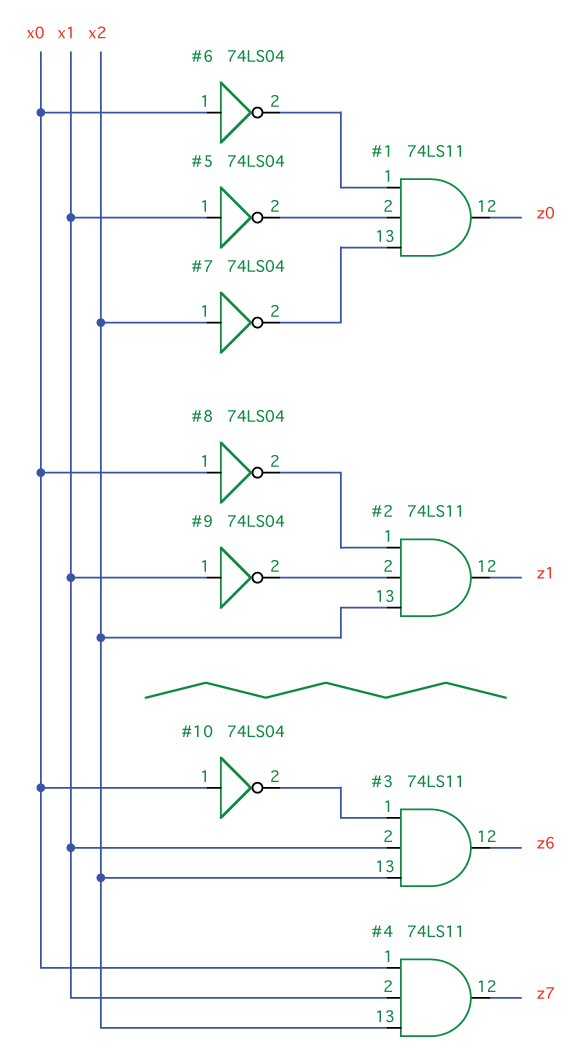
Figure 3.50 Decoder with Gates
Summary
We've covered a lot of ground in this chapter. Each layer—digital logic, microcomputer, and software—can stand on its own, so there's no need to be too concerned if you didn't grasp everything. It doesn't mean you won't be able to understand the upcoming chapters. If you'd like to learn even more about digital logic, I would encourage you to look at the following list of resources:
Books:
- The Art of Electronics by Horowitz and Hill (Cambridge University Press, 1989)
- Hands-On Electronics by Kaplan and White (Cambridge University Press, 2003)
On the Internet:
- CAL for Digital Logic: http://www.ee.surrey.ac.uk/Projects/Labview/
- Digital Logic: http://www.play-hookey.com/digital/
- Discover Circuits: http://www.discovercircuits.com/D/digital.htm
- How Electronic Gates Work: http://electronics.howstuffworks.com/digital-electronics.htm
- TTL Data Book: http://upgrade.cntc.ac.kr/data/ttl/
| ← Previous | Contents | Next → |